A Printed Circuit Board, or PCB, is a module that supports and connects electronic components. The circuits on a PCB are formed from a conductive material, such as copper foil, deposited onto a non-conductive substrate. The individual electronic components of the circuit are then soldered onto the conductive material.
PCBs can be single-sided, double-sided, or multi-layered, depending on how many components are required for the circuit. Most electronic products will contain a Printed Circuit Board, but how are they manufactured?
The Printed Circuit Board manufacturing process
The first step of the PCB manufacturing process is to make the substrate. The substrate is created by combining woven glass fibre and epoxy resin and then rolled into the desired thickness. The substrate is then semi-cured in an oven and cut into panels. These panels are stacked in alternating layers with adhesive copper foil. These layers are then pressed under high temperatures, bonding the copper foil to the substrate.
When a double-sided or multi-layered PCB is being manufactured, holes must be drilled to electrically connect the circuits on the different sides or layers. To do this, holes are drilled and deburred in the determined pattern in the circuit boards and these holes are then lined with copper to create a conductive connection.
The next step is to create the printed circuit pattern, which is done by plating copper upon the substrate, and then a layer of positive photoresist material is vacuumed onto the foil surface. The printed circuit pattern mask is placed on top and exposed to UV light so that the photoresist material within the circuit pattern becomes soluble.
The circuit pattern mask is then removed, and the panel is sprayed with an alkaline developer, leaving the copper foil circuit pattern exposed. The panels are electroplated with copper and then another protective coating is added on top of this to stop the copper from oxidising.
After the circuit pattern has been created, contact fingers are attached to the edge of the substrate and masked off and then plated with metals. These contact fingers are used to attach the board to other PCBs or external electrical devices.
The panels are then sealed with epoxy to protect the circuits and are then cut to individual boards. At this stage, any necessary markings or instructions are also stencilled onto the board.
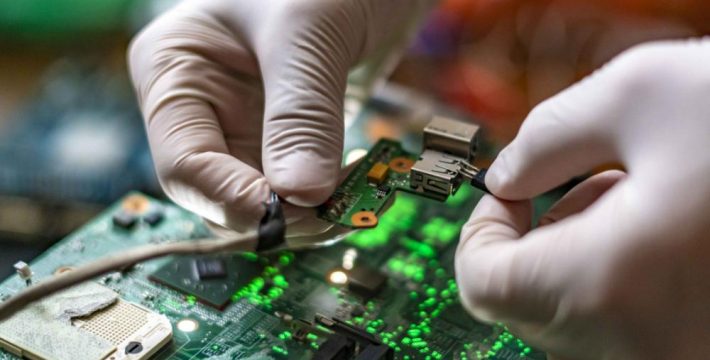
The final stage of printed circuit board manufacturing is to mount the components. Some components will be soldered into place by a machine, such as a chip shooter for smaller components or robotically placed for larger components, but very large or irregularly shaped components will need to be placed and soldered manually.
Printed Circuit Board services
One of the big advantages of PCBs is that it is cheaper and faster to mass produce them than it is for other circuit wiring methods because the layout only needs to be created once and components are mounted to the circuit and wired together in one operation. For this reason, PCBs are well suited for high-volume production, but they can also be manufactured in small batches and for prototype purposes.
The best manufacturers of printed circuit boards go above and beyond and will provide a full design service as well as production. This begins by creating a schematic diagram and then using CAD/CAM software before manufacture begins to design the circuit layout and component placement.
Manufacturers who offer a complete PCB service will also be able to reverse engineer PCBs. Some older PCBs may need replacing due to faults or damage but may also have been made using older components that are no longer readily available. Reverse engineering the board allows it to be rebuilt but using newer components, to perform the same function as before, and possibly to a higher level of performance.
Here at Delta Impact, we have over 25 years of experience in supplying high-quality PCBs. If you are looking for PCBs in high-volume, small-batch, or prototype capacity, you can find out more about our Printed Circuit Board services.